Engineers:- Emerging AI applications, like chatbots that generate natural human language, demand denser, more powerful computer chips. But semiconductor chips are traditionally made with bulk materials, which are boxy 3D structures, so stacking multiple layers of transistors to create denser integrations is very difficult.
As humans have gotten more and more dependent on computers for life and work, the need for more powerful and denser computer chips has gotten greater. This is especially true with emerging AI applications including ChatGPT -like chatbots. Now, researchers at the Massachusetts Institute of Technology (MIT) have developed a new technology that could help us build much more denser circuits on computer chips.
In the past, researchers have grown 2D materials elsewhere and then transferred them onto a chip or a wafer. This often causes imperfections that hamper the performance of the final devices and circuits. Also, transferring the material smoothly becomes extremely difficult at wafer-scale. By contrast, this new process grows a smooth, highly uniform layer across an entire 8-inch wafer.

‘Growing’ transistors on a Silicon wafer
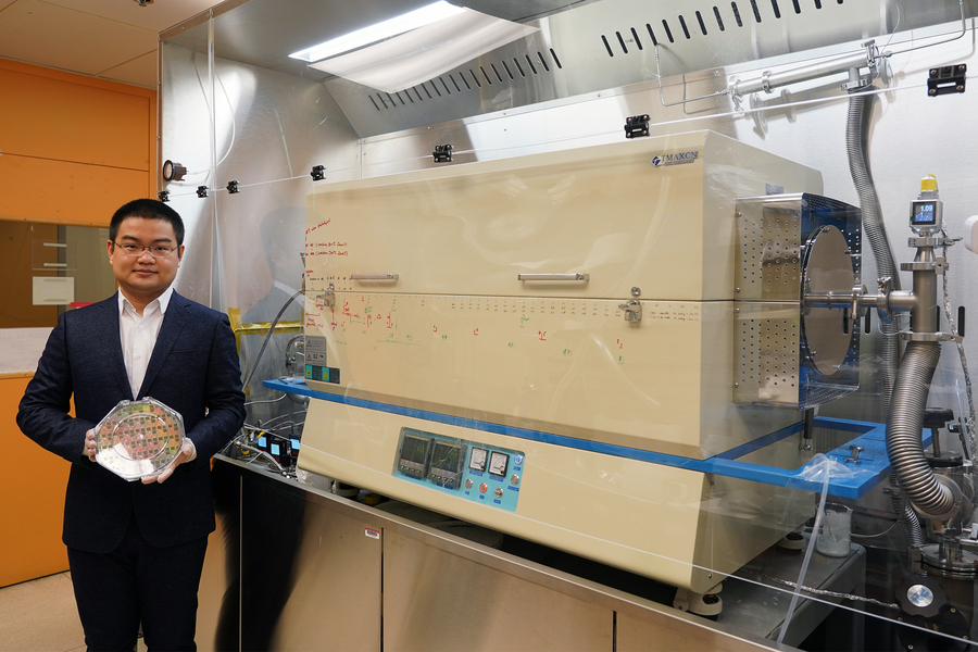
With the new method, the engineers “grew” layers of 2D transition metal dichalcodenide materials on a fully fabricated silicon chip. In the past, researchers have tried growing 2D materials elsewhere and transferring them onto a chip or a wafer but this could cause imperfections that can impede the performance of devices.
Slim materials with vast potential
The 2D material the researchers focused on, molybdenum disulfide, is flexible, transparent, and exhibits powerful electronic and photonic properties that make it ideal for a semiconductor transistor. It is composed of a one-atom layer of molybdenum sandwiched between two atoms of sulfide
Problems with the process
Silicon circuits usually have aluminium or copper as a top layer so that the chips can be connected to a “carrier” before it is mounted on a circuit board. But the sulphur in diethylene sulphur, one of the organic molecules used in the process, sulphurises these metals. This is similar to how metals rust when they are exposed to oxygen, affecting their conductivity.
But the new technology consists of a relatively low-temperature growth process that does not damage the fully-fabricated chip. This tech can be used to directly integrate 2D semiconductor transistors on top of standard silicon circuits, according to MIT. This process can be used to grow a smooth, highly uniform layer across an 8-inch wafer, without the issues that come with growing the layer elsewhere and integrating it into the circuit.
Faster growth and better uniformity
One problem with this process is that silicon circuits typically have aluminum or copper as a top layer so the chip can be connected to a package or carrier before it is mounted onto a printed circuit board. But sulfur causes these metals to sulfurize, the same way some metals rust when exposed to oxygen, which destroys their conductivity. The researchers prevented sulfurization by first depositing a very thin layer of passivation material on top of the chip. Then later they could open the passivation layer to make connections.

The future of the technology:- Engineers
The researchers now plan to fine-tune their technique so that many stacked layers of 2D transistors can be grown in the future. Along with this, they also want to see how this low-temperature growth process can be adapted to flexible surfaces like polymers, textiles, or even papers. According to MIT, this could mean that semiconductors can be integrated into objects like clothing and notebooks.
“This work made an important progress in the synthesis technology of monolayer molybdenum disulfide material,” says Han Wang, the Robert G. and Mary G. Lane Endowed Early Career Chair and Associate Professor of Electrical and Computer Engineering and Chemical Engineering and Materials Science at the University of Southern California, who was not involved with this research. “The new capability of low thermal budget growth on an 8-inch scale enables the back-end-of-line integration of this material with silicon CMOS technology and paves the way for its future electronics application.”
This work is partially funded by the MIT Institute for Soldier Nanotechnologies, the National Science Foundation Center for Integrated Quantum Materials, Ericsson, MITRE, the U.S. Army Research Office, and the U.S. Department of Energy. The project also benefitted from the support of TSMC University Shuttle.


